
Project 07 – Exploring fundamental growth morphologies in organic thin film systemsChristian Teichert, ao.Univ.Prof.Dr. Exploring fundamental growth morphologies in organic thin film systems aims a deeper understanding of the growth mechanisms of organic thin film systems. Primarily based on atomic force microscopy, we will quantitatively study the growth front evolution of molecular thin films (like sexiphenylene, sexithiophene, pentacene, phthalocyanine) on different – mainly crystalline – substrates as a function of coverage and growth parameters. The emphasis will be on a comparative study of two fundamentally different growth techniques available within the NFN: OMBE and HWE. Quantitative pattern analysis of both, in situ AFM investigations of UHV growth experiments and ex situ studies of samples grown by the partners, will yield information on size, shape and arrangement of the organic nanostructures. The evolution of these parameters will allow to reveal the underlying diffusion mechanisms, the driving forces for the observed ordering phenomena, and the relation between molecular orientation and resulting surface morphology. In situ growth experiments using LEEM and XPEEM/LEEM are planed to verify the proposed growth models. The results should allow - in conjunction with results of the partner groups - to optimize the deposition of ordered molecular films with interface controlled properties.
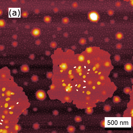
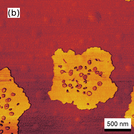 AFM height image of a 1.3 nm thick 6P film grown on a modified mica(001) surface. Corresponding phase image to (a) revealing that the large 6P islands grow directly on the modified mica surface. PRESS RELEASEUnusual Nanoscale Mound Formation Terrace-like elevations of just a few nanometres can form during production of organic thin films made from electrically conductive material. This phenomenon was previously only known from inorganic materials and is crucially important for future production of a new generation of semi-conductor components based on organic thin films. The data now published in the first July edition of SCIENCE was collated as part of a national research network funded by the Austrian Science Fund FWF. Inorganic semi-conductors have a simple construction and have made high-performance computers possible. In contrast, organic semi-conductors are complex but enable production of innovative electronic circuits, as vividly demonstrated by the first prototypes for roll-up screens. Yet these benefits of organic semi-conductors can only be fully harnessed when the response of their organic molecular layer – whose thinness is crucial in functional terms – is better understood. The national research network (NRN) “Interface controlled and functionalised organic thin films” of the Austrian Science Fund FWF is contributing to precisely this understanding. Microscopic Height Measurement In the latest issue of SCIENCE, a team from the NRN has now been able to show that organic molecules spread out on a carrier material in a previously unknown form to create thin electrically conductive films. As Prof. Christian Teichert from the Institute of Physics at the University of Leoben explains: "Totally surprising diffusion behaviour at step edges formed during film growth was observed on the films of the organic substance parahexaphenyl produced by solid state physicists from Graz University of Technology. The molecules here come into contact with a diffusion barrier, which leads to the other molecules piling up. Although a diffusion barrier of this nature is well known in inorganic, atomically structured films – it is called the Ehrlich-Schwoebel barrier in honour of its inventors – it had not previously been observed for organic materials." The team in Leoben used scanning force microscopy to better understand this hitherto unknown behaviour of the organic molecules. This enabled precise measurement of the nano mounds at the step edges. Evaluation of the data thus obtained led to a further surprise. The shape of the nano elevations is strongly reminiscent of the terraced mounds encountered in mining. The team was struck by the fact that the terrace height of 2.6 nm almost exactly matches the length of a molecule of parahexaphenyl. The conclusion from this is that the molecules align themselves upright within a terrace. However, it was also shown that the lower terraces are somewhat lower in height than those above. Project team member Dr. Gregor Hlawacek explains this phenomenon: "The data from the measurement allowed us to calculate the Ehrlich-Schwoebel barrier for this case. It also transpired that the molecules of the lower terraces are deposited at an angle. As a result, the terrace height here diminishes relative to the angle of inclination." Energy-saving Measure at Nano Level The measured values were used to perform computer simulations in the Chair of Atomistic Modelling and Design of Materials. These were not only able to confirm the experimental values for the diffusion barriers but also revealed that the parahexaphenyl molecules are bent in diffusion. This was surprising as bending requires expansion of the bonds in the molecule, which is in fact avoided owing to the energy required. However, in this way, the diffusing molecule can maintain bonds to neighbouring molecules more effectively than a rigid molecule, so that bending is overall the more energy-saving mechanism. For the team from Leoben and Graz, these findings are extremely exciting as producing organic thin-film transistors requires closed films of such upright molecules. Improved understanding of the fundamental forces that bring this about will enable them to be manipulated and thus used in a controlled way. This NRN is therefore making a direct contribution to the future production of a new generation of semi-conductor components. Text and image material available from 08:00 GMT on Wednesday 09.07.08 at: englisch http://www.fwf.ac.at/en/public_relations/press/pv200807-en.html Original publication: Characterization of Step-Edge Barriers in Organic Thin-Film Growth, G. Hlawacek, P. Puschnig, A. Winkler, C. Ambrosch-Draxl & C. Teichert. Science (2008), 108-111. Scientific contact: FWF Austrian Science Fund: Editor/publisher: Vienna, 08 July 2008 |


Page last modified on August 26, 2008, at 11:16 PM