
|
There is an enormous world-wide effort both in basic scientific research as well as in industrial development in the area of organic electronics. It is becoming increasingly clear that, if devices based on organic materials are ever going to have a significant relevance beyond being a cheap replacement for inorganic semiconductors, there will be a need to understand interface formation, film growth and functionality. A control of these aspects will allow the realisation of totally new device concepts exploiting the enormous flexibility inherent in organic chemistry. In the field of device-relevant “semiconducting” organic materials one finds many parallels with that of inorganic semiconductors. However, the versatility of organic molecules comes at the cost of higher materials complexity. This rules out the simple transfer of concepts established from inorganic semiconductor research, and makes work on organic semiconductors particularly challenging. World-wide, investigations into organic thin films can be partitioned into three areas of focus with different aims and mixes of applied versus basic research: (1) the development and production of devices, (2) thin film characterisation and more recently, with the recognition of the importance of molecular level control (3) surface and interface science. The vision of the NFN partners is that functional organic molecules can be the basic building blocks for both low cost large area and new nanoscale devices, ranging from solar cells to chemical sensors. Because of the technological relevance and the applications that can be imagined for devices incorporating organic films it is important to understand the fundamental processes of organic film formation, the structures that are formed, their interfaces and their properties. In this NFN homogeneous films, organic heterostructures and prototypes of selected key devices are to be simulated, fabricated and characterised. The conceived NFN with its multidisciplinary character bridging the gap from the surface to the device, is, therefore, well placed to make a significant impact on steering future research on organic electronics. Linking these branches will create enormous synergies leading to a significant advance in the field of organic semiconductors. Eventually it will result in the development of the tools for tuning device properties on a nanoscopic level. This will ensure that Austrian science stays at the forefront of basic research in this emerging technology. 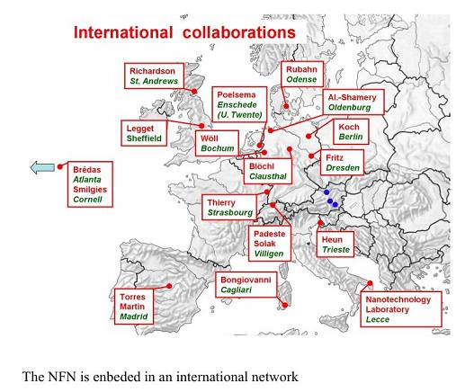 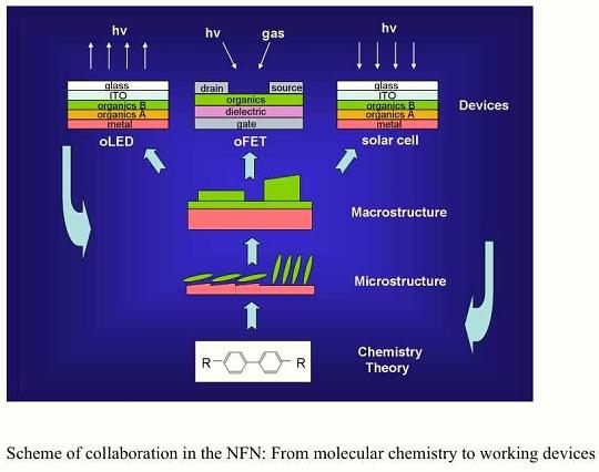 |


Page last modified on August 13, 2008, at 06:48 PM